 |
|
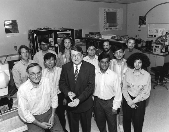
Eric Fossum and the team that invented the CMOS image sensor, at NASA’s Jet Propulsion Laboratory. Image credit: NASA/JPL-Caltech |
Eric Fossum, the celebrated inventor of the modern CMOS sensor and longtime friend of DPReview, recently appeared on the B&H Photography Podcast to reminisce on his work at NASA’s Jet Propulsion Laboratory (JPL) on the invention of the CMOS image sensor in 1993, its surprising origins and his years-long attempts to convince US manufacturing companies to use it for consumer goods.
It’s not an overstatement to say his technology changed the world. We may look at our smartphones, turn on the TV, or use a webcam for virtual meetings. When we leave our homes, we may back a car out of a parking space with a backup camera, be seen by security cameras or be captured in the background of social media videos. A CMOS image sensor makes these devices possible in each of these instances.
The funny thing is, this father of modern photography didn’t even care much for the medium growing up.
“I enjoyed it, but I wouldn’t say I was fascinated by it,” Fossum said about cameras and photography during his youth.
To put it into context, Fosum was born in October 1957 (the same month Sputnik was launched, but more on that later), and picture-taking was an expensive endeavor. He recalled his parents giving him permission to use the family’s Kodak Brownie to take a picture on rare occasions and then just one, saying things like, “Okay, today is Wednesday; you can take another picture.”
A 1958 TV commercial from 1958 for the Kodak Brownie camera.
Today, he takes pictures more freely. One friend has described him as a postcard photographer, to which Fossum responded that he isn’t quite sure if that is an insult or a compliment.
“Not a day goes by where the world doesn’t interact with the technology Fosssum created.”
Fossum’s journey toward reinventing how we think of cameras and imaging began with a fascination with science and space. He was born the same month and year Russia launched Sputnik and grew up with the space race it spawned.
From playing with toy rockets and propulsion techniques as a child, he later went on to play with the real thing with a Howard Hughes Fellowship. The fellowship allowed him to work on missile guidance systems at the Hughes Aircraft Company in California over three summers.
There, he worked on a project that was starting to place cameras into missile heads to help the missile hit its intended target. That set him down a path into electronics, and by the mid-80s he was teaching electrical engineering at Columbia University. Space was still of interest to him, but his work in electronics had taken him down a different path and he had resigned himself to it.
The Sputnik satellite was launched the same month Fossum was born, kicking off the space race that influenced his youth and interest in space and science.
While teaching, he was also researching CCD technology and focal plane image processing. The metaphysical nature of photons as a wave and a particle also made it fun to think about. “I had been thinking about image sensors,” he recalled. “But decided who needs it?”
Then NASA came knocking.
The US space agency was aware of his work and wanted to develop cheaper and faster cameras that could survive in space long term. “All of a sudden, when it became clear that what I was working on was of interest to NASA, I was just like, oh yeah, sign me up,” Fossum said. “They didn’t have to ask twice.”
Fossum joined NASA’s JPL in 1990, and with their support, he began the development of CMOS image sensors. He showed NASA how the technology was superior to CDD for space travel: CMOS cameras would require less power to operate, they could be smaller in form factor without the additional parts CCD required, and fewer parts mean less weight and fewer things that could break down, and they were better at withstanding the cosmic rays of space than CCD.
 |
|
A CMOS active pixel image sensor chip fits on a fingertip. Image credit: NASA/JPL-Caltech |
It also helped that CMOS was a technology already being used to manufacture integrated circuits for many electronics, and the infrastructure to build a CMOS image sensor was already in place.
“It was really that driver. I was able to argue why we had to … explore CMOS image sensor technology, and NASA invested in that,” Fossum said. “(That’s) why you have a camera in your pocket right now.”
Fossum is also quick to point out he didn’t do it alone. “All engineers stand on the shoulders of the giant engineers that came before us,” he remarks several times during the interview. His work was built on the pioneering work of generations before him and the teams that worked with him.
 |
| The stacked CMOS sensors of the Nikon Z9 are a descendant of the first CMOS sensors created in the 1990s. |
The whole story is worth a listen: Fossum details the science of light, the first products to use CMOS image sensors and some lovely breakdowns of how CCD and CMOS sensors capture images.
Not a day goes by when the world doesn’t interact with the technology Fossum created. It’s as ubiquitous a part of our modern life as a father talking about the weather or a DPReview editor tinkering with new gear.


