10 years ago Canon announced they had purchased Austin Texas’s Molecular Imprints Inc, and this was a purchase that I who is always looking at the tech side of Canon was excited about. I was very interested in seeing if Canon could make something with this technology. It had an insane amount of promise at the time.
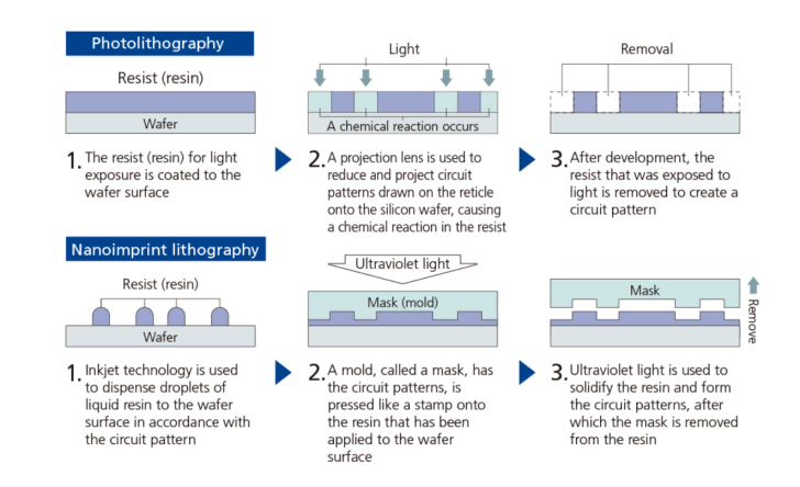
First, we should do a brief outline of the difference between nanoimprint lithography (NIL) and regular photolithography machines.
A normal photolithography machine can be simplistically explained as it beams light through a large pattern that is reduced in size by optics onto the resin that is coated on a semiconductor blank wafer. This light causes a chemical reaction to occur in the resin. Then resin that was hit with the 1light is removed by a process called etching. These entire steps are repeated multiple times as there are many layers to a modern chip. For modern lithography machines, the technology needed to do this is simply insane.
Nano Imprinting (NIL) is different than the normal photolithography process because instead of etching the conductive resin away, the design is imprinted onto the wafer. The process uses precision drops of resin and a mold to place the resin in the chip patterns on the wafer, this resin forms the conductive circuit patterns on the wafer without the need to etch the resin away.
Nanoimprint is a simpler process and requires a far less complex machine therefore lower machine cost than photolithography and since NIL doesn’t need a high-powered laser doing some downright crazy EUV (extreme ultraviolet) magic (you have to take a read on how this is done and the incredible amount of research needed) the entire process saves a ton of power as well.
From Canon, we see their comparison of the two technologies.

But it’s not all good things with NIL. NIL has to have a very precise alignment which is quite difficult to do as it needs to press each layer onto the wafer on top of one another to form the semiconductor. Any misalignment can ruin the entire chip. This is far less of a problem with photolithography. Also, the resin droplets have to be incredibly precise in size according to the design layout of the chip. NIL is considered to be only suitable now for producing less complex semiconductors, primarily for this reason.
So no matter how neat NIL sounds photolithography is not entirely going away as the photolithography process has been refined and improved over many decades. They are still able to produce chips that are far more complex than what NIL can do. Canon themselves suggest that NIL machines will augment fabrication plants but not entirely replace the traditional lithography machines in use today.
Canon goes into a lot of the technologies and what they have done over the years to improve the technology from their original purchase of Molecular Imprints all the way back from 2004 here. It’s a good read but would cause too many eyes to water, including my own, going into the full detail here. I believe this page was published by Canon in 2019, and updated since, making it pretty relevant to how the current machines developed by Canon are operating. Canon also has created a good summary video on the technology and how it works.
Canon also suggests that producing chips this way is far easier on the environment and costs, with savings of up to 90% of the power consumption and 50% of the costs against current EUV machines.
Canon has recently done two announcements that have caused a stir (and led to me writing all this). Reading all the news on this has been slightly confusing and there is obviously a ton of politics and related hysteria involved with this as well. I’m not going to delve into the hysteria and that particular mess with the exception of stating that these machines are a lot easier to fabricate and copy if someone wanted to. Whereas an EUV lithography machine requires high-tech parts and equipment that are extremely difficult to recreate without leading-edge technologies across multiple technology and optical disciplines. Of course, Canon has a bazillion patents on this technology, so this obviously can’t be done legally but that may not be an issue in some instances.
On October 4th, Nikkei Asia reported that Canon has plans to build a new 50 billion yen (345 million USD) plant in the Tochigi prefecture that will begin production of the NIL machines in 2025. Canon hopes that the new plant will double the current production of lithography machines. According to Nikkei, Canon expects a 29% rise in sales year on year, which would also be a 400% increase from 10 years ago. This new plant along with the existing two current plants is expected to meet the increased demand for equipment. Canon expects the new plant to allow for a doubling of current production. Nikkei doesn’t mention the equipment, but they do suggest that the equipment is for cutting-edge fine-circuit semiconductors. This would lead me to believe that Canon expects to manufacture primarily NIL equipment there.
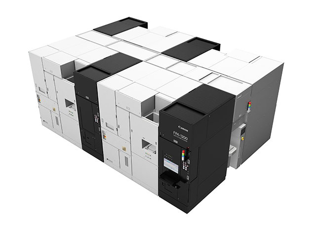
Then later, a few days ago on October 13th, Canon announced (again) the FPA-1200NZ2C lithography NIL machine. It can achieve down to the equivalent of 5nm node designs, and Canon also expects that with further mold refinement in the future, these machines will be able to get down to a comparable node size of 2nm which will make it competitive with the most advanced lithography equipment in use today.

The first FPA-1200NZ2C was actually in production and shipping to Toshiba Memory Corporation and was announced back in 2017. I did note that at the time Canon suggested “patterns” down to 10nm on the machine which I will assume meant equivalent node size since that is always smaller than line widths, and hey, they are trying to brag. So it would appear as if Canon spent the last 5+ years perfecting and continuing the development of the platform with Toshiba as they are now claiming an equivalent node size down to 5nm and further refinement down to 2nm. However, no details were given by Canon on what transpired or was improved from the time of the first FPA-1200NZ2C machine delivery and now. I am going to presume that some of the advancements that Canon discusses were done after the first deployment.
Canon currently controls around 30% of the lithography market. ASML is the dominant player with 60% of the lithography market. But that’s not as good as it sounds right now for Canon. Because ASML controls all of the advanced lithography done with EUV. These machines from ASML manufacture all the advanced semiconductors for flash memory, RAM, CPU, GPU, and AI chips. Basically, any advanced IC right now is using ASML machines. The other players such as Canon sell machines that fill the needs that don’t require EUV machines (usually DUV – Deep Ultraviolet) such as discrete components and smaller-scale ICs.
Canon with the development of the new factory is betting on its increased market share in the lithography field with this equipment and supplanting the need for EUV to develop all of the advanced semiconductors. So in the future, Canon has a vision where their NIL machines will manufacture all your flash memory and various other advanced semiconductors alongside ASML’s EUV machines.
Hopefully, with this equipment being developed and sold to fabrication plants, Canon will help achieve lower costs for bulk ICs such as flash memory. With cheaper SSDs, we could see a significant lowering of the cost per terabyte of SSDs down to a level even closer to that of physical HDDs. Something we can all get behind.
Some of our articles may include affiliate links. If you purchase through these links, we may earn an affiliate commission at no extra cost to you.


